STM32 CAN Bus Dev Board PCB Design | Part 1 – Schematic Design
Автор: PajoPCB
Загружено: 2026-01-12
Просмотров: 78
Join My Skool Community:
https://www.skool.com/pcb-learning-co...
STM32 CAN Bus Development Board | EP4 Part 1 – Schematic Design
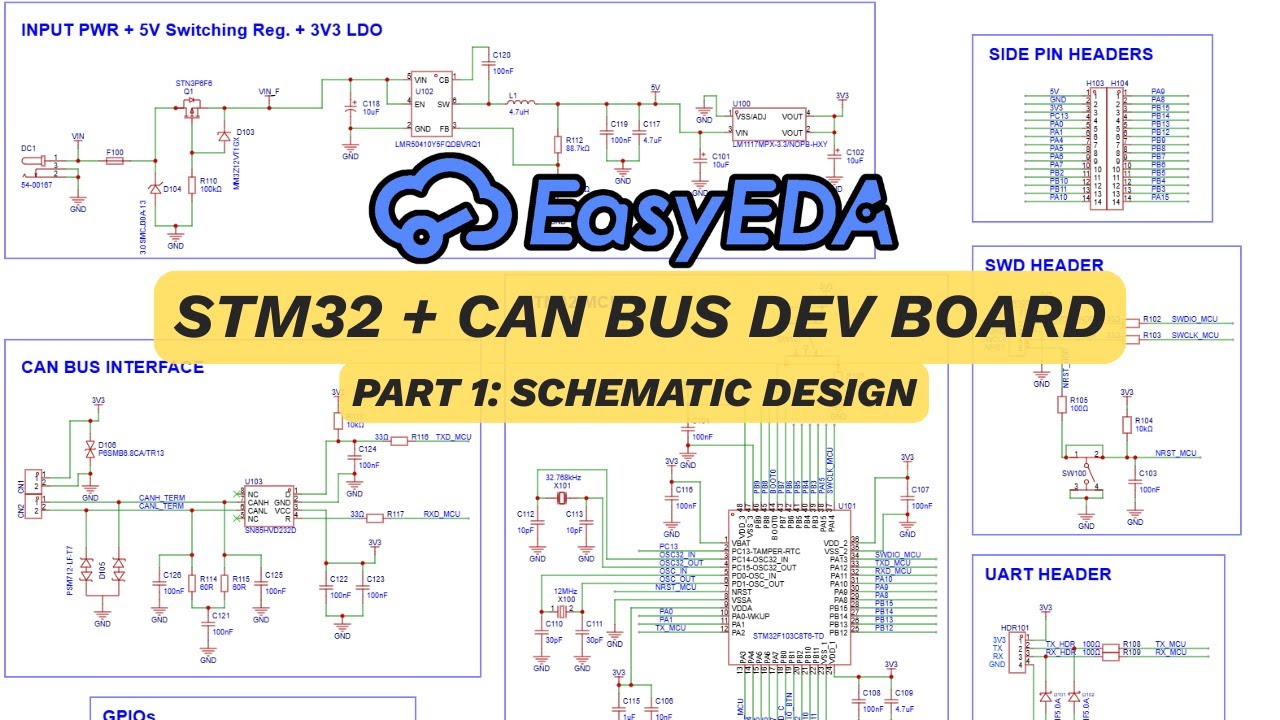
In Episode 4 of the STM32 development board series, we design an STM32-based CAN bus development board, starting with the schematic design.
This video is Part 1 of the project and focuses entirely on the electrical design and system architecture. We go through each section of the schematic step by step, explaining not just what is connected, but why it’s designed this way.
In this episode, we cover:
Overall system architecture and block diagram
Wide-input power design (7–24V) with protection circuitry
Buck regulator and low-noise 3.3V LDO strategy
CAN transceiver interface with TVS protection and split termination
UART, SWD, BOOT0, reset, and debug circuitry
GPIO buttons, LEDs, and exposed headers
Clocking, decoupling, and MCU bring-up essentials
The goal of this video is to build a robust, real-world schematic suitable for noisy environments where CAN is commonly used, such as automotive and industrial applications.
Доступные форматы для скачивания:
Скачать видео mp4
-
Информация по загрузке:


