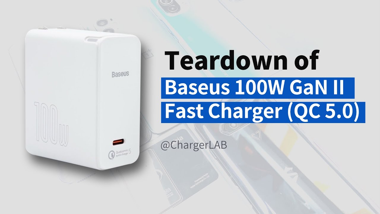
Teardown of Baseus 100W GaN II Fast Charger (QC 5.0)
Автор: ChargerLAB
Загружено: 2021-08-20
Просмотров: 17215
You can buy it on Amazon: https://amzn.to/3sCdcya
If you wanna buy the tester of POWER-Z, you can visit our Amazon store:
https://www.amazon.com/s?me=A31UM8SRX...
Introduction
---------------------------------------------------------------
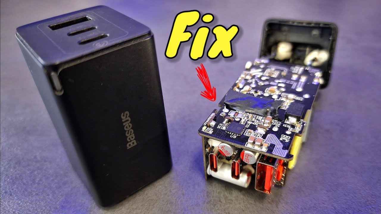
Hi, guys. Today, ChargerLAB will disassemble the Baseus 100W GaN II Fast Charger with QC5.0 protocol, the world’s first QC5 100W GaN charger.
At the same time, the charger is also compatible with QC2.0 and QC3.0 and other protocols.
Then, we’ll see each part of this new QC5 fast charger.
If you think our video is helpful, please subscribe to our channel for more content.
Bill of materials
---------------------------------
PFC boost controller: ON Semiconductor NCP1622BEC
PFC boost switching transistor: Navitas NV6125 (GaN MOSFET)
High-frequency PWM controller: ON Semiconductor NCP1342
High voltage switching MOSFET: Oriental Semiconductor OSG65R200J
Synchronous rectifier controller: Meraki Integrated MK91808
Synchronous rectifier MOSFET: Hunteck GN093N12SL
Protocol chip: Injoinic IP2726S
VBUS switching transistor: ZMJ ZM027N03N
Chapter
----------------------------------
0:00 Intro
1:09 Size and Performance
1:44 Teardown - Start
3:10 Teardown - Components
6:37 Teardown - Output Board
7:24 Summary
For more details. You can visit our website:
https://www.chargerlab.com
SOCIALS:
Instagram: / chargerlabs
Facebook: / chargerlab
Twitter: / chargerlab
For Business Inquiries: info@chargerlab.com
Доступные форматы для скачивания:
Скачать видео mp4
-
Информация по загрузке: