Скачать
8086 General Bus Operation Timing Diagram | Memory Read & Write Cycle.
Автор: ASN Vision
Загружено: 2025-12-28
Просмотров: 48
Описание:
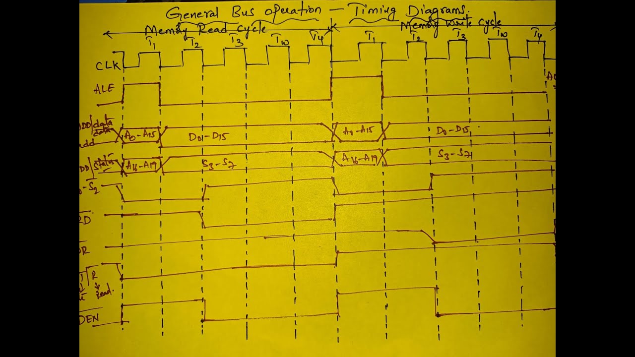
In this video, we clearly explain the 8086 General Bus Operation Timing Diagram, covering both Memory Read Cycle and Memory Write Cycle.
You will understand the role of CLK, ALE, RD, WR, DEN, AD0–AD15, A16–A19, and status signals S0–S7 with proper timing waveforms.
This explanation is very useful for:
ECE students
Microprocessors & Microcontrollers (8086)
GATE & University exams
Interview preparation
Watch till the end for an easy and exam-oriented understanding of 8086 bus timing diagrams.
Доступные форматы для скачивания:
Скачать видео mp4
-
Информация по загрузке:


