Скачать
ASUS GTX 580 DirectCU II Teardown and PCB Overview
Автор: CmdrSoyo
Загружено: 2019-11-16
Просмотров: 2422
Описание:
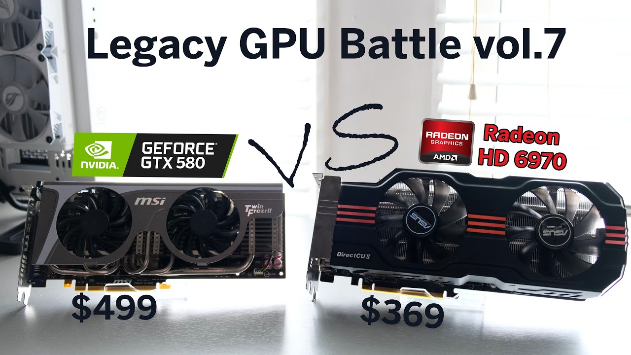
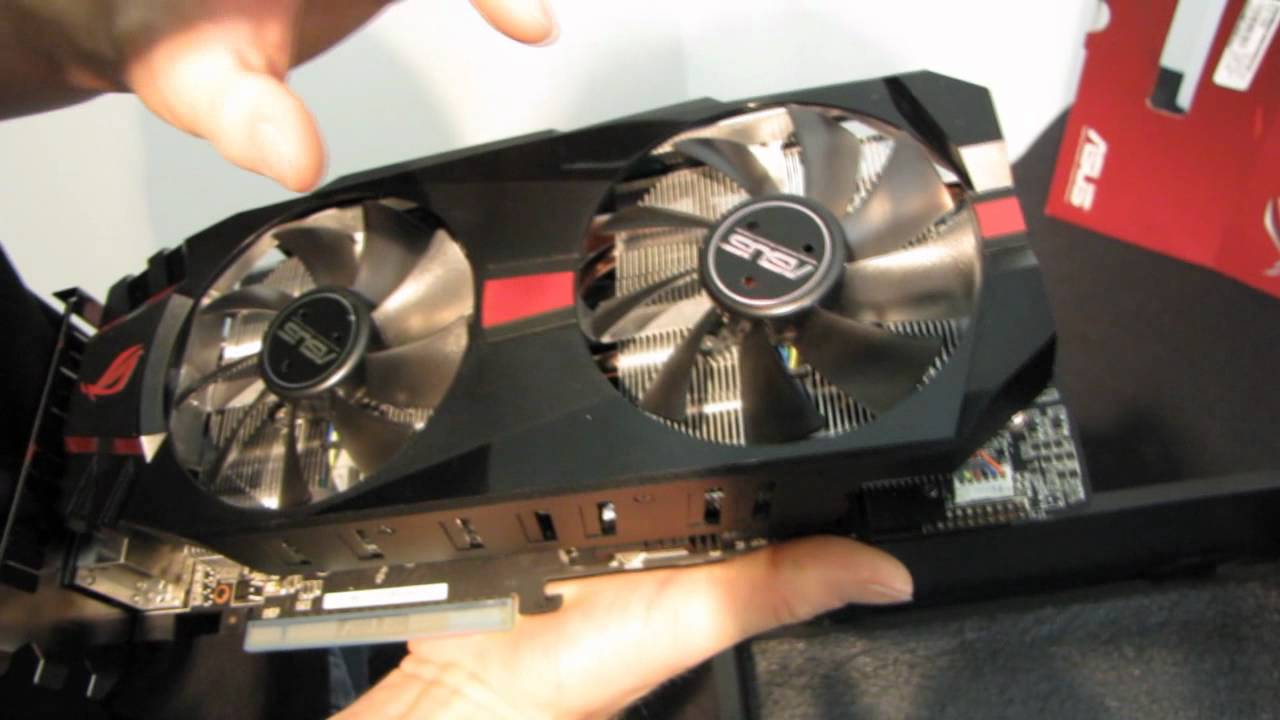
Today we take a look at my (very old) ASUS GTX 580's PCB and overall design/construction by tearing it down and looking at what's inside...
Timestamps:
0:00 Intro
1:01 Shroud Removal
2:46 Fan Assembly Removal
4:34 Main Heatsink Removal
5:59 Additional Talk about the Fans
7:35 Main Heatsink Overview
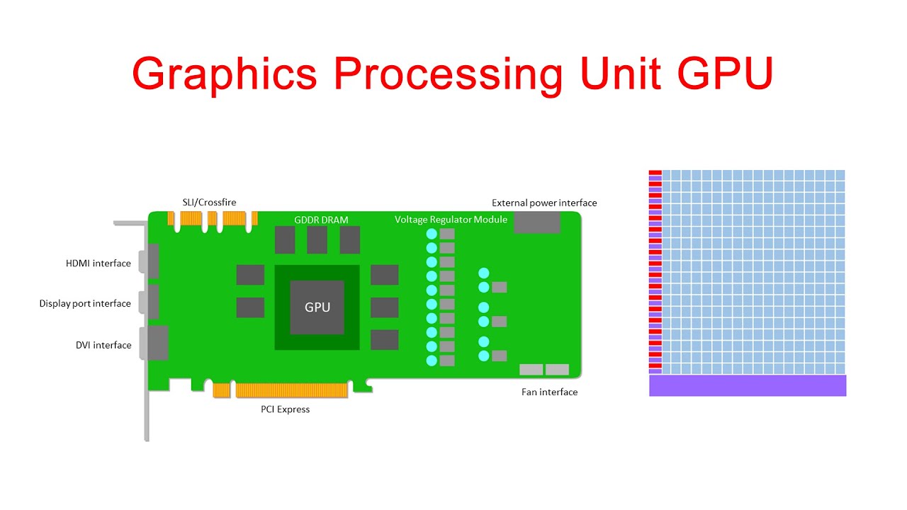
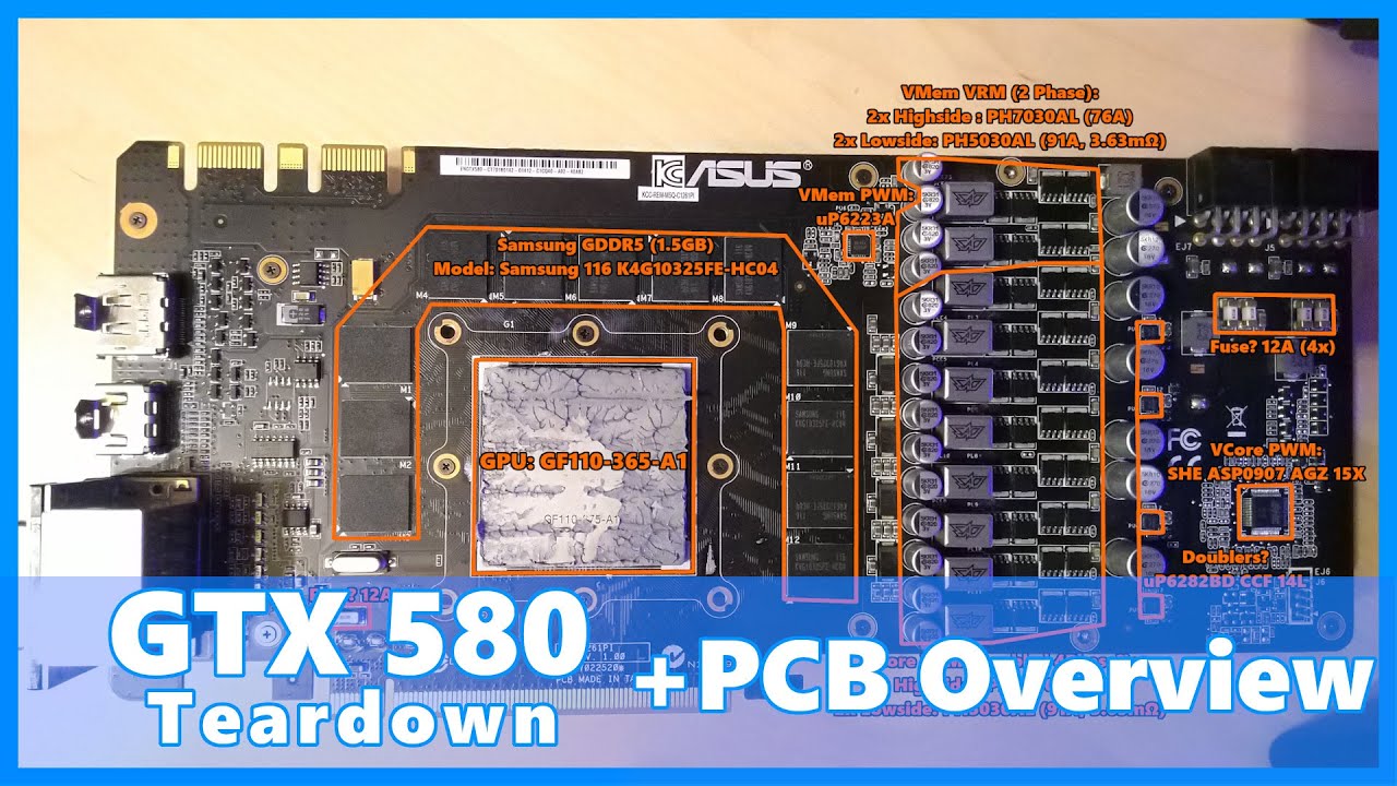
8:45 PCB Overview
9:57 VRM Overview
13:34 Fuses and theoretical max Power consumption
14:42 Cleaning the GPU
17:00 Talking about the "Proadlizer" Capacitor
note: the GTX 480 actually has 480 Shader Units not 385 as i said in the video... that's a screw-up on my part, sorry
Thanks for watching! Comments aswell as Likes/Dislikes are appreciated.
Доступные форматы для скачивания:
Скачать видео mp4
-
Информация по загрузке: