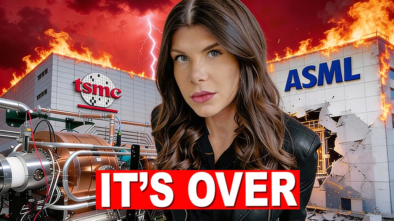
Why ASML & TSMC Chip Factories Are Scared of This Tiny American Startup!
Автор: Evolving AI
Загружено: 2026-01-19
Просмотров: 1093
Until now, advanced chips have belonged to a tiny club: TSMC prints almost all of the world’s leading-edge silicon, and ASML’s $400–500 million EUV scanners are the only tools that can pattern them. This video examines the first serious challenge to that model: a U.S. startup called Substrate, which is eliminating EUV from the equation and betting everything on compact X-ray lithography instead. Their machine uses a built-in particle accelerator to generate ultra-short-wavelength X-rays, stamping features in a single shot instead of relying on expensive multi-patterning—and they’ve already shown 12 nm features with High-NA-class precision at a fraction of the tool cost. We’ll break down how Substrate’s approach could cut lithography tool prices from ~$500M to ~$50M, why that matters when fabs are heading toward $50B builds and $100,000 wafers, and why the company doesn’t want to sell tools at all, but build its own U.S. foundry to directly compete with TSMC and Samsung. We also examine rival accelerator-based light source efforts, such as xLight, and why most of them still rely on ASML rather than replace it. Is this the start of an entirely new chipmaking era—or a brutal reminder of how unforgiving high-volume manufacturing really is? And if you want the real story behind the world’s fastest-moving AI and semiconductor breakthroughs, make sure to like and subscribe to Evolving AI for daily coverage.

Доступные форматы для скачивания:
Скачать видео mp4
-
Информация по загрузке: