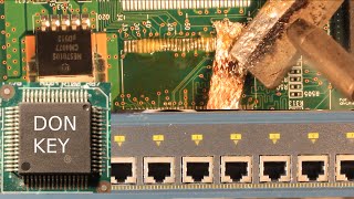
Cisco 2960G Switch teardown an detailed overview for CCNA lab and repair -Part2
Автор: Donkey Learning IT
Загружено: 2016-02-06
Просмотров: 14031
Complete tear-down and overview of a Cisco 2960G gigabit switch for CCNA candidates and also for IT repair technicians.
At the first half of the video I go over the main components which are the Flash, NVRAM, Route-Processor and ASIC from the perspective of a CCNA. On the CCNA exam you do not need to know such details, but it helps you to be able to visualize the data flow, and to give you a rough idea about the hardware.
In the secon half of the video I go over the mainboard components in deep detail, and explain their functionality within the Switch. This part is going way beyond CCNA, instead it caters for component-level repair technicians.
If you are interested in the disassembly and the PSU, watch Part1 of this video series:
• Cisco 2960G Switch teardown an detailed ov...
Some portions of ot the video got lost because of the Kdenlive Linux video editor, sorry for the choppy video.
Parts list for the Mainboard discussed in the video:
====================================
Route Processor: Cisco Yeti2 (IBM Power-PC 405 core + FPGA)
Flash: Intel TE28F128
NVRAM: Flash emulated (no dedicated chip)
RAM: Micron 46V32M16 64MB DDR modul
TCAM table: Renases R8A20300ABG
ROMMON I could not find the chip holding the boot-ROM
Serial Console: MB3232I
ASIC from Cisco
Parts list for the other components:
====================================
U67 IR 0901 A6P3N6 (is there a datasheet?)
U76=U77 Maxim 8566E
U67=U66 Maxim 8643E
U64 ISL8700IBZ
U46=U61=U2 SN74LVC245A
U70=U32=U33=U34 SN54HC595
U7=U83 P149FCT20807HE
U81 ADTT75A
U6 CY2CC8100-XT1
U84 UD8808265 (is there a datasheet?)
U54=U53 SN74LVC126A
Q20 NE47810S DDR Double Data Rate linear regulator
U14 MB3232I
U82=U68=U69=U47=U48 7Z25L = NC7SZ125M5X

Доступные форматы для скачивания:
Скачать видео mp4
-
Информация по загрузке:


![Почему взрываются батарейки и аккумуляторы? [Veritasium]](https://ricktube.ru/thumbnail/a3-3R9zwyGY/mqdefault.jpg)