LayTec's EpiX Animation: Follow an epi-wafer on its path through the EpiX station
Автор: LayTec AG
Загружено: 2024-01-26
Просмотров: 615
With LayTec’s EpiTT, EpiCurve®TT & Pyro 400 #insitu #metrology for #epitaxy, EpiX C2C Mapping Station for Epi-wafers, and TRIton in-situ #EPD metrology for plasma #etching, all your critical frontend processes are assisted and guided by LayTec metrology. With our Connected Metrology, wafer-specific measurements are combined to enable a new level of compound semi process control.
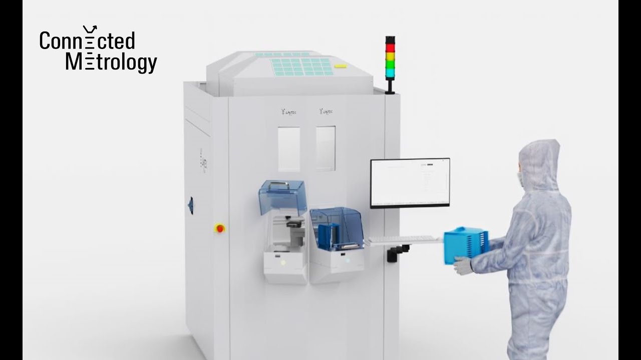
Let’s have a look in detail, how the #EpiX Mapping Station contributes to this process: The EpiX C2C tool is a cassette-to-cassette white light reflectance and photoluminescence mapping station for compound semi production epi-wafers, be it device structures based on GaN, GaAs, InP or any other compound #semiconductor material.
With its unmatched low spectral noise, absolute accuracy and 2D measurement homogeneity, it renders precise analysis results that enable classification on the die-level.
Additionally, using wafer-specific EpiNet® MOCVD epitaxy analysis results, even complex device stacks can be analyzed to obtain the 2D profiles of critical layer thicknesses and compositions. These results, in turn, are used to facilitate sub-nm precision endpointing with LayTec in-situ metrology for plasma etching.
Reach out to info@laytec.de for more info on this topic!
Доступные форматы для скачивания:
Скачать видео mp4
-
Информация по загрузке:


