Популярное

Музыка Кино и Анимация Автомобили Животные Спорт Путешествия Игры Юмор

Интересные видео

2025 Сериалы Трейлеры Новости Как сделать Видеоуроки Diy своими руками

Топ запросов

смотреть а4 schoolboy runaway турецкий сериал смотреть мультфильмы эдисон
dTub
Скачать

Circuit Board Layout for EMC: Example 3

Автор: LearnEMC

Загружено: 2015-03-06

Просмотров: 41687

Описание:

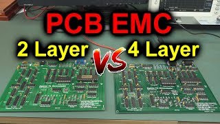
This printed circuit board does not meet the FCC Class B radiated EMI requirements. In this example we'll redesign this layout so that radiated and conducted emissions requirements are easily met. We'll also improve immunity to radiated and conducted interference.

Circuit Board Layout for EMC: Example 3

Поделиться в:

Доступные форматы для скачивания:

Скачать видео mp4

  • Информация по загрузке:

Скачать аудио mp3

Похожие видео

Circuit Board Layout for EMC: Example 2

Circuit Board Layout for EMC: Example 2

EEVblog #1176 - 2 Layer vs 4 Layer PCB EMC TESTED!

EEVblog #1176 - 2 Layer vs 4 Layer PCB EMC TESTED!

Circuit Board Layout for EMC: Example 1

Circuit Board Layout for EMC: Example 1

9 Simple Tricks to Improve EMC / EMI on Your Boards - Practical examples (with Min Zhang)

9 Simple Tricks to Improve EMC / EMI on Your Boards - Practical examples (with Min Zhang)

Introduction - PCB design for good EMC

Introduction - PCB design for good EMC

Lecture 1: Sampling, anti-alias filter, oversampling, reconstruction; Into to Quantization

Lecture 1: Sampling, anti-alias filter, oversampling, reconstruction; Into to Quantization

#002 SMPS Design for Low EMI (How to Pass Conducted Emissions Testing)

#002 SMPS Design for Low EMI (How to Pass Conducted Emissions Testing)

(Спонсируется) Советы по проектированию оборудования/печатных плат со смешанными сигналами — Лабо...

(Спонсируется) Советы по проектированию оборудования/печатных плат со смешанными сигналами — Лабо...

Power Distribution Tips To Control SI, EMI and Noise-Rick Hartley

Power Distribution Tips To Control SI, EMI and Noise-Rick Hartley

3 Basic Tricks For EMC Compliant PCB Layout

3 Basic Tricks For EMC Compliant PCB Layout

005 DC-DC Converter Layout - Solid Ground Plane or Cutout Below Switch Node?!

005 DC-DC Converter Layout - Solid Ground Plane or Cutout Below Switch Node?!

PCB Layout Fundamentals

PCB Layout Fundamentals

Introduction to Basic Concepts in PCB Design

Introduction to Basic Concepts in PCB Design

Learn To Fix EMC Problem Easily And In Your Lab - Troubleshooting Radiated Emissions | Min Zhang

Learn To Fix EMC Problem Easily And In Your Lab - Troubleshooting Radiated Emissions | Min Zhang

What your Differential Pairs Wish You Knew with Rick Hartley - AltiumLive Keynote

What your Differential Pairs Wish You Knew with Rick Hartley - AltiumLive Keynote

Простое руководство по электронным компонентам.

Простое руководство по электронным компонентам.

RF & Analog Mixed Signal PCB Design

RF & Analog Mixed Signal PCB Design

High Speed and RF Design Considerations

High Speed and RF Design Considerations

Заземленные плоскости с питанием и смешанными сигналами

Заземленные плоскости с питанием и смешанными сигналами

Switching Power Supply PCB Layout Seminar

Switching Power Supply PCB Layout Seminar

© 2025 dtub. Все права защищены.


  • Контакты
  • О нас
  • Политика конфиденциальности


Контакты для правообладателей: [email protected]