How Are Chips Made? | The Secret World of EDA & IP
Автор: Cadence Design Systems
Загружено: 2026-01-20
Просмотров: 2213
Behind every smartphone and AI there is a world of software called EDA. Discover how chips are designed using Cadence tools, from logic gates to multi-die chiplets.
Every modern system is a harmony of hardware and software. But have you ever wondered how those billions of transistors on a tiny chip actually get there? The answer is Electronic Design Automation (EDA). It is the sophisticated software that designers use to build the brains of our devices. At Cadence, we live at the heart of the EDA and IP business, providing the building blocks that turn a designer's vision into a physical reality. It’s a journey that starts with a single logic gate and evolves into systems with billions of connections.
In the semiconductor world, "IP" isn't just about patents; it stands for Intellectual Property (IP) in Electronics. Think of IP as pre-designed, standardized pieces of a chip — like a ready-to-use engine for a car.
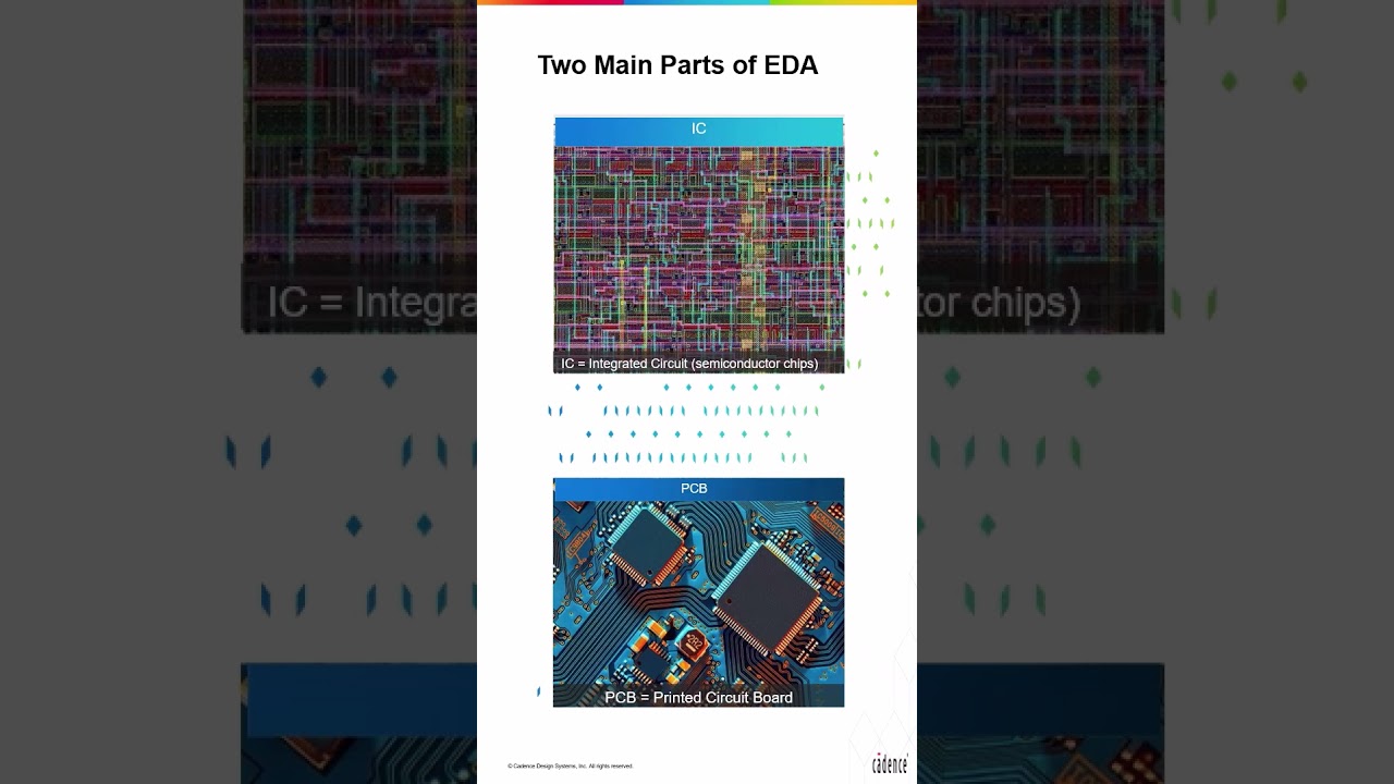
EDA Tools: The "workshop" where the design happens, covering IC and PCB Design.
Soft IP (RTL): Standardized specifications that allow designers to integrate complex functions in a shorter time.
Hard IP (Layout): Pre-designed physical blocks ready for the chip's "map."
Frequently Asked Questions (FAQ) :
1. What does EDA stand for?
It stands for Electronic Design Automation, the software used for designing semiconductor chips and full systems.
2. What is IP in this context?
In electronics, IP refers to pre-designed chip blocks that help designers bring products to market faster.
3. What are chiplets?
Chiplets and Multi-Die Systems involve integrating multiple dies within a single package to handle the incredible complexity of modern electronics.
Timestamps :
0:12 – Defining the role of EDA software in chip design
0:36 – Why modern design includes package board and enclosure modeling
0:48 – Explaining IP as the building blocks beyond the logic gate
1:05 – The difference between RTL (soft IP) and Layout (hard IP)
1:26 – The evolution from simple gates to billions of gates in IC design
1:45 – Transitioning from single die to multi-die chiplet configurations
---------------------------------------------------------------------------------------------------------------------------------------------------------------
Connect with Cadence :
• YouTube: / @cadencedesignsystems
• LinkedIn: / cadence
• Facebook: / cadencedesign
• Twitter/X: / cadence
• Instagram: / cadencedesignsystems
---------------------------------------------------------------------------------------------------------------------------------------------------------------
About Cadence :
Cadence is a global leader in electronic systems design, applying its Intelligent System Design™ strategy to deliver software, hardware, and IP that turn design concepts into reality.
Cadence® customers are among the world’s most innovative companies, creating breakthrough products — from chips to boards to full systems — across markets including hyperscale computing, 5G, automotive, aerospace, mobile, consumer, industrial, and healthcare.
Recognized by Fortune as one of the 100 Best Companies to Work For ten (10) consecutive years.
Learn more at https://www.cadence.com.
#eda #semiconductors #intelligentsystemdesign
Доступные форматы для скачивания:
Скачать видео mp4
-
Информация по загрузке:


![Как происходит модернизация остаточных соединений [mHC]](https://imager.clipsaver.ru/jYn_1PpRzxI/max.jpg)


