KiCad Zones/Copper Planes Tutorial - (Part 1/2)
Автор: Kicad Tutorials
Загружено: 2016-10-17
Просмотров: 58634
Please see part 2 of the tutorial on how to remove soldermask/copper: • Removing Soldermask and Copper Fill (Part ...
Click "Show More" for Timestamps/Video Chapters
Let me know if anything is wrong in the tutorial and I'll try and update it, along with anything you'd like covered. The Kicad docs are not bad, but watching the video is still recommended.
Kicad Docs: http://docs.kicad-pcb.org/stable/en/p...
Edit: looks like I forgot to mention how to make non-copper planes...I guess that one's for next time. In short, select a non-copper layer, then press the 'make plane button' as normal, which will then bring up the special dialog, as shown at the beginning of the video.
[Timestamps]
00:00 - Introduction
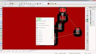
00:23 - Creating ground planes
02:13 - Clearance Settings
03:30 - Corner Smoothing
04:00 - Overlapping Zone / Zone Priorities
05:51 - Pad Connection Types / Thermal Relief
06:00 - "Solid" and "Thermal Relief" Connection Types
06:53 - Throughole "THT Thermal" and "None" Connection Types
07:40 - Individual Pad Relief Settings
08:29 - Whole Footprint Relief Settings
09:05 - Unconnected planes do not fill
10:02 - Via Stitching (WARNING: Kicad 5 has dedicated via button! Don't use this method, use the via button on the right toolbar instead)
10:25 - DRC Error - Zones Too Close
12:12 - Kicad bug with xone extending past zone area with corner smoothing (Not sure if Kicad 5 has fixed this)
13:00 - "Hidden Pins" on Schematic Symbols
13:45 - Tip: Regenerating Zones before Export (NOTE: I think Kicad 5 now warns you about this!)
15:20 - Merging Zones Together
15:58 - Keep-out Zones (No Fill Zones)
End of Video - But see part 2 for removing soldermask/copper: • Removing Soldermask and Copper Fill (Part ...

Доступные форматы для скачивания:
Скачать видео mp4
-
Информация по загрузке: