EEVblog
Автор: EEVblog
Загружено: 2016-11-02
Просмотров: 292528
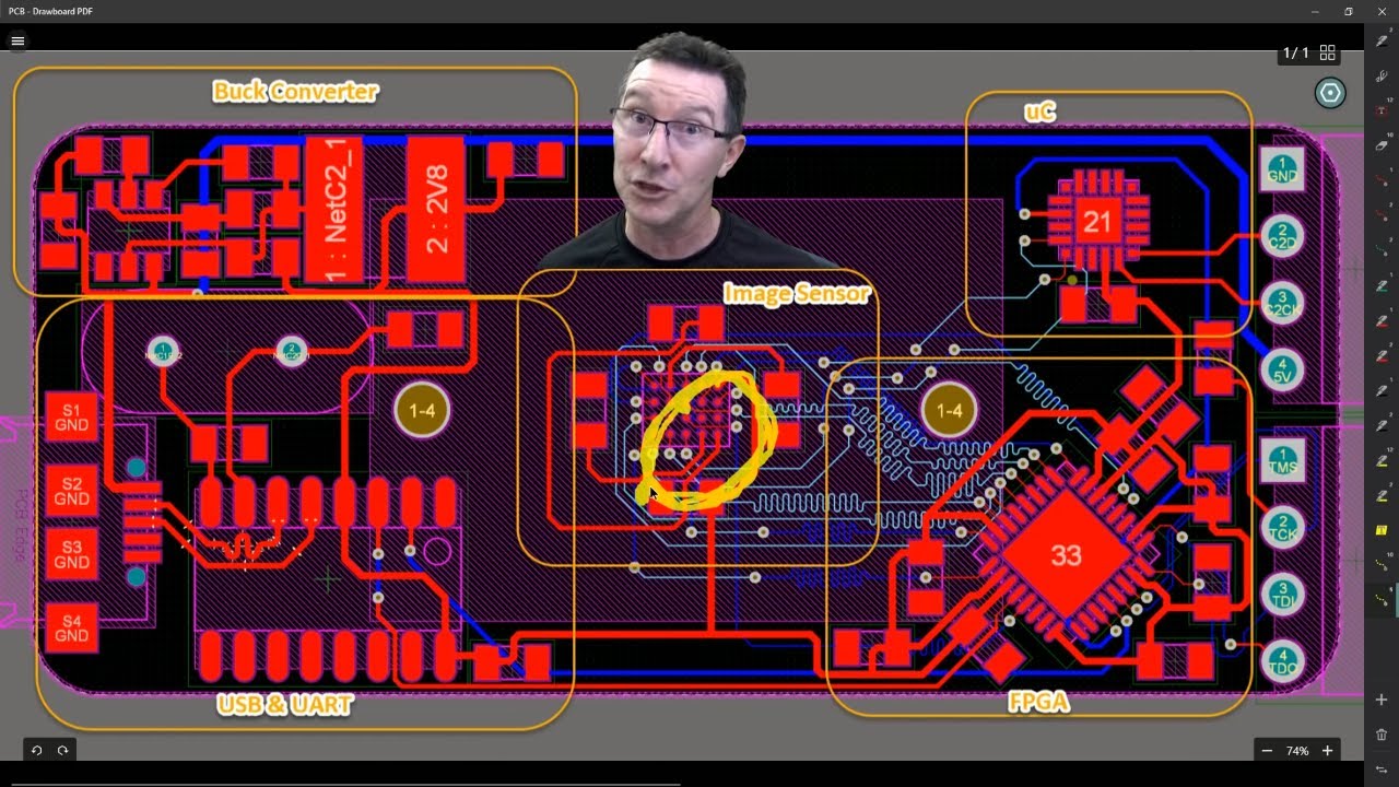
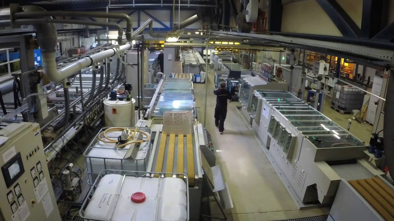
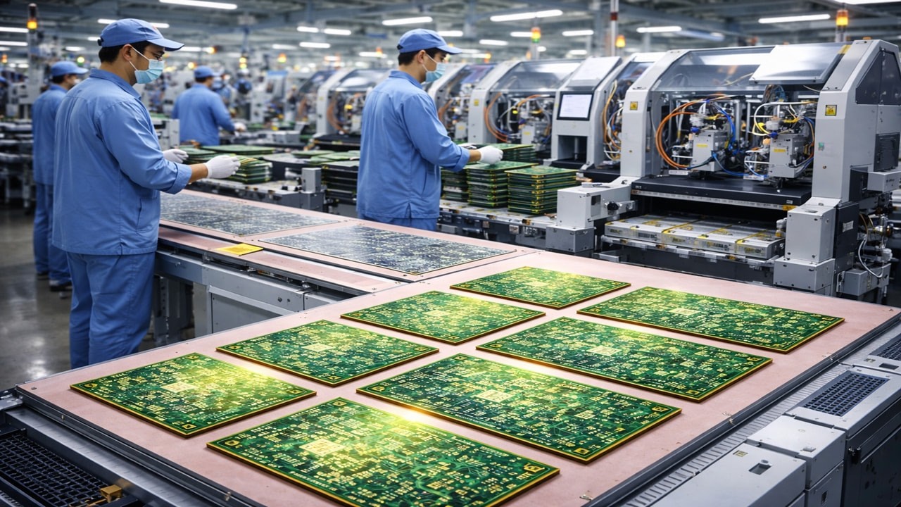
How is a double sided plated through hole solder masked and silk screened component olverlay PCB manufactured?
Take a step-by-step tour of a PCB manufactuing plant.
http://www.pcbzone.net
Forum: http://www.eevblog.com/forum/blog/eev...
Hard electroplated gold card edge connectors: • Part 20 - Plated gold edge connectors
Desing for manufacture tutorial: • EEVblog #127 - PCB Design For Manufacture ...
DFM Automated PCB Panel Testing: • EEVblog #552 - DFM Automated PCB Panel Tes...
Alba PCB Group Video: • Direct Imaging, for your PCB printing / Di...
Eurocircuits Video: • Part 17 - RoHS compliant surface finishes ...
EEVblog Main Web Site: http://www.eevblog.com
The 2nd EEVblog Channel: / eevblog2
Support the EEVblog through Patreon!
/ eevblog
EEVblog Amazon Store (Dave gets a cut):
http://astore.amazon.com/eevblogstore-20
T-Shirts: http://teespring.com/stores/eevblog
💗 Likecoin – Coins for Likes: https://likecoin.pro/@eevblog/dil9/hcq3

Доступные форматы для скачивания:
Скачать видео mp4
-
Информация по загрузке: