Популярное

Музыка Кино и Анимация Автомобили Животные Спорт Путешествия Игры Юмор

Интересные видео

2025 Сериалы Трейлеры Новости Как сделать Видеоуроки Diy своими руками

Топ запросов

смотреть а4 schoolboy runaway турецкий сериал смотреть мультфильмы эдисон
dTub
Скачать

PCB Design: Top Factors Related to Data Routing and Layout

Автор: Epec Engineered Technologies

Загружено: 2025-04-10

Просмотров: 312

Описание:

When it comes to PCB design and layout, the decisions made early in your project can significantly impact not only the functionality of your circuit board but also its manufacturability, cost, and lead time. Understanding these critical considerations helps ensure a seamless transition from design to production while avoiding costly errors or delays.

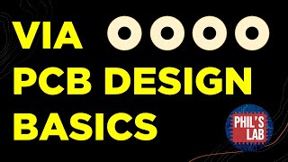
Key factors to address include material selection, maximum board thickness, layer count, and whether to incorporate advanced features like blind and buried vias.

Additionally, considerations around copper weights, trace widths and spacing, balanced copper distribution, and overall design complexity can heavily influence both manufacturability and reliability.

A crucial question is: When should you involve your PCB provider in the design process? Engaging early can help identify potential roadblocks, ensure design-for-manufacturing (DFM) compatibility, and optimize your layout for efficient production.

In this webinar, we take a deep dive into PCB designs as they relate to manufacturing. Whether you’re developing a simple two-layer board or a complex multilayer design, this session will provide actionable insights to streamline your process and achieve the best results for your project.

For more information on our PCB solutions, visit https://www.epectec.com/pcb.

PCB Design: Top Factors Related to Data Routing and Layout

Поделиться в:

Доступные форматы для скачивания:

Скачать видео mp4

  • Информация по загрузке:

Скачать аудио mp3

Похожие видео

How to Properly Size and Select Your Custom Flexible Heater

How to Properly Size and Select Your Custom Flexible Heater

(Sponsored) PCB Vias 101 - Phil's Lab #77

(Sponsored) PCB Vias 101 - Phil's Lab #77

In the Age of AI: Why Asking Questions Matters More Than Finding Answers | Dr. Shivendu S.

In the Age of AI: Why Asking Questions Matters More Than Finding Answers | Dr. Shivendu S.

Understanding UL Wire Options that Surpass Industry Standards

Understanding UL Wire Options that Surpass Industry Standards

How to route USB data lines on a PCB

How to route USB data lines on a PCB

PCBA Design Decisions and SI/EMC Consequences

PCBA Design Decisions and SI/EMC Consequences

KiCad Tutorial | Beginning to End

KiCad Tutorial | Beginning to End

(Sponsored) 2-Layer PCB Design Tips - Phil's Lab #137

(Sponsored) 2-Layer PCB Design Tips - Phil's Lab #137

БЕЛЫЕ СПИСКИ в России: разбираю 7 VPN-протоколов — какие ещё работают?

БЕЛЫЕ СПИСКИ в России: разбираю 7 VPN-протоколов — какие ещё работают?

Сшивание с помощью Deep Dive | Разводка печатной платы

Сшивание с помощью Deep Dive | Разводка печатной платы

Мужик украл карася, Муму и Герасим, Участковый Сюткин, У губ твоих конфетный вкус - КВН ДАЛС

Мужик украл карася, Муму и Герасим, Участковый Сюткин, У губ твоих конфетный вкус - КВН ДАЛС

Два инженера соревнуются в разработке печатной платы всего за час! Кто победит?

Два инженера соревнуются в разработке печатной платы всего за час! Кто победит?

Лазер и Фрезер 2 в 1 - Идеальный ЧПУ по цене телефона!

Лазер и Фрезер 2 в 1 - Идеальный ЧПУ по цене телефона!

6 Horribly Common PCB Design Mistakes

6 Horribly Common PCB Design Mistakes

🧪🧪🧪🧪Как увидеть гиперпространство (4-е измерение)

🧪🧪🧪🧪Как увидеть гиперпространство (4-е измерение)

How To Design and Manufacture Your Own Chip

How To Design and Manufacture Your Own Chip

Где начало СХЕМЫ? Понимаем, читаем, изучаем схемы. Понятное объяснение!

Где начало СХЕМЫ? Понимаем, читаем, изучаем схемы. Понятное объяснение!

(Sponsored) How To Improve Your PCB Designs (Common Mistakes) - Phil's Lab #18

(Sponsored) How To Improve Your PCB Designs (Common Mistakes) - Phil's Lab #18

Автотрассировщик KiCAD 7 — простое и быстрое прототипирование

Автотрассировщик KiCAD 7 — простое и быстрое прототипирование

High Speed PCB Design Rules (Lesson 4 of Advanced PCB Layout Course)

High Speed PCB Design Rules (Lesson 4 of Advanced PCB Layout Course)

© 2025 dtub. Все права защищены.


  • Контакты
  • О нас
  • Политика конфиденциальности


Контакты для правообладателей: [email protected]