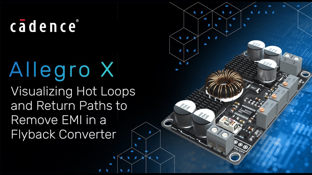
Visualizing Hot Loops and Return Paths to Remove EMI in a Flyback Converter
Автор: Cadence PCB Design and Analysis
Загружено: 2026-01-12
Просмотров: 223
Struggling with EMI issues in your flyback or switch-mode power supply? In this video, Kirsch breaks down why flyback converters often fail EMI testing and, more importantly, how to fix the issue using PCB layout techniques that require no additional components. You’ll learn how hot loops and broken return paths are the primary culprits behind high electromagnetic emissions, and how to minimize them with component placement, copper pours, and return path strategy. With a real-world PCB layout example in Allegro X, this tutorial provides actionable design tips that you can apply immediately to your power converter designs.
Check out other videos on Power Supply in Allegro X: • Avoid Power Converter Pitfalls: EMI, Simul...
Try Allegro X free for 30 days: http://bit.ly/4qKn0D7
Subscribe to our Channel: / @cadencepcbdesignandanalysis
Follow us on social for the latest OrCAD X news!
👉 Follow Cadence PCB Design and Analysis on X: / cadencesda
👉 Follow Cadence PCB Design and Analysis on LinkedIn: / cadencesda
👉 Follow Cadence PCB Design and Analysis on Facebook: / cadencesda
Disclaimer: This video may have been recorded prior to changes made to the product’s user interface, or the video may be based on an earlier release of the product. The concepts and workflows conveyed in this video still apply to the current release of the product.

Доступные форматы для скачивания:
Скачать видео mp4
-
Информация по загрузке:


