Скачать
How to Create a PCB Footprint in Altium Designer | Step-by-Step Tutorial-In Hindi
Автор: PCB Playground
Загружено: 2025-12-30
Просмотров: 38
Описание:
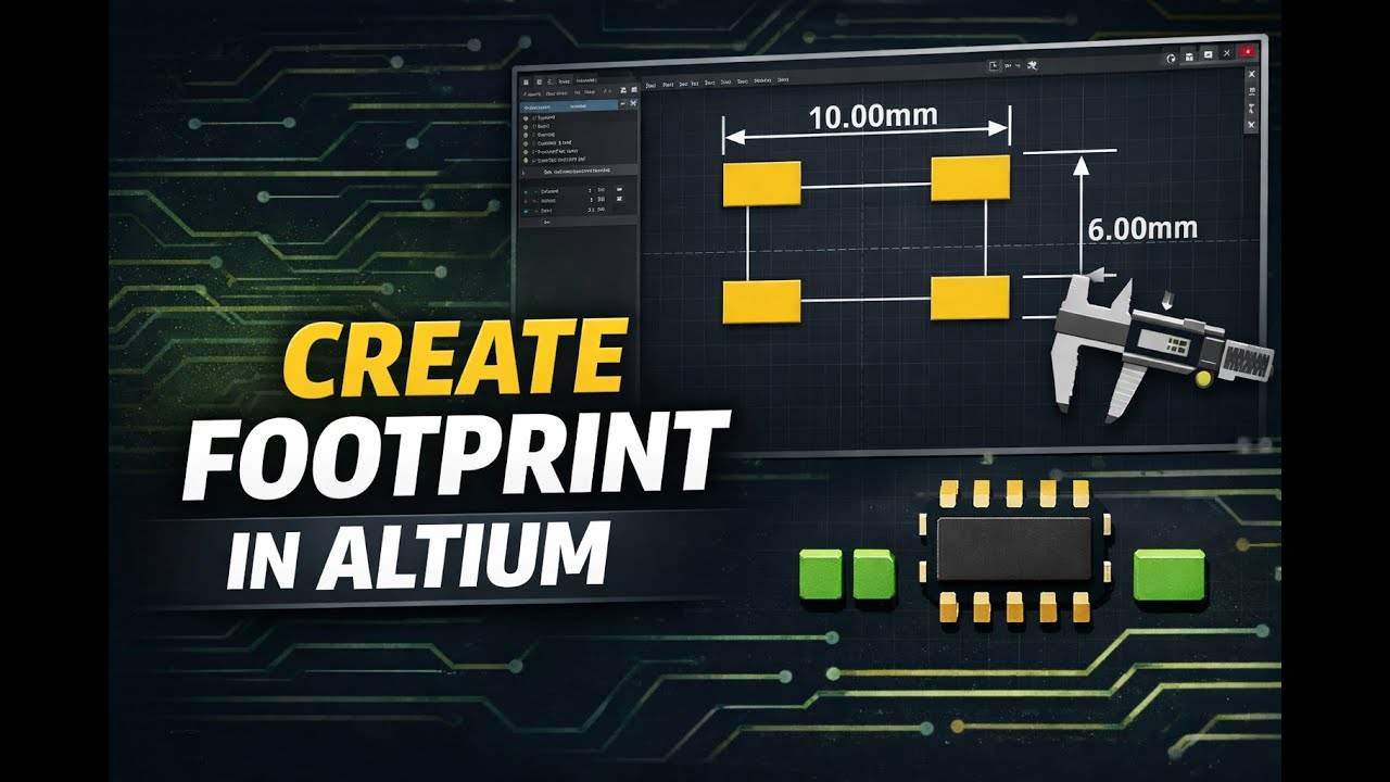
In this video, I explain how to create a PCB footprint in Altium Designer step by step.
You will learn how to design accurate SMD and through-hole footprints, set correct pad sizes, spacing, and dimensions, and follow industry-standard PCB design practices.
This tutorial is perfect for:
✔ Beginners learning Altium Designer
✔ PCB designers & electronics engineers
✔ Students working on PCB projects
By the end of this video, you’ll be confident in creating custom footprints for any component in Altium Designer.
Доступные форматы для скачивания:
Скачать видео mp4
-
Информация по загрузке: