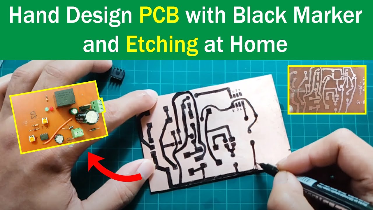
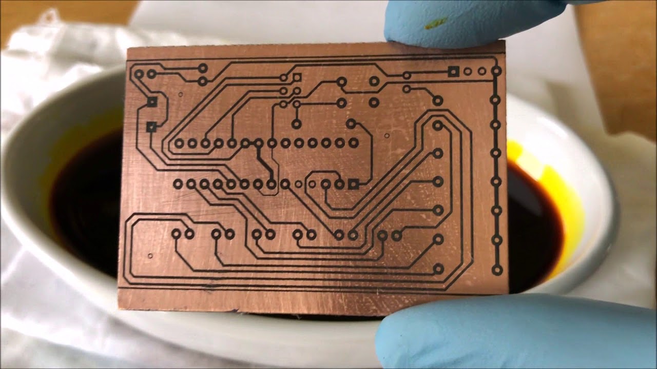
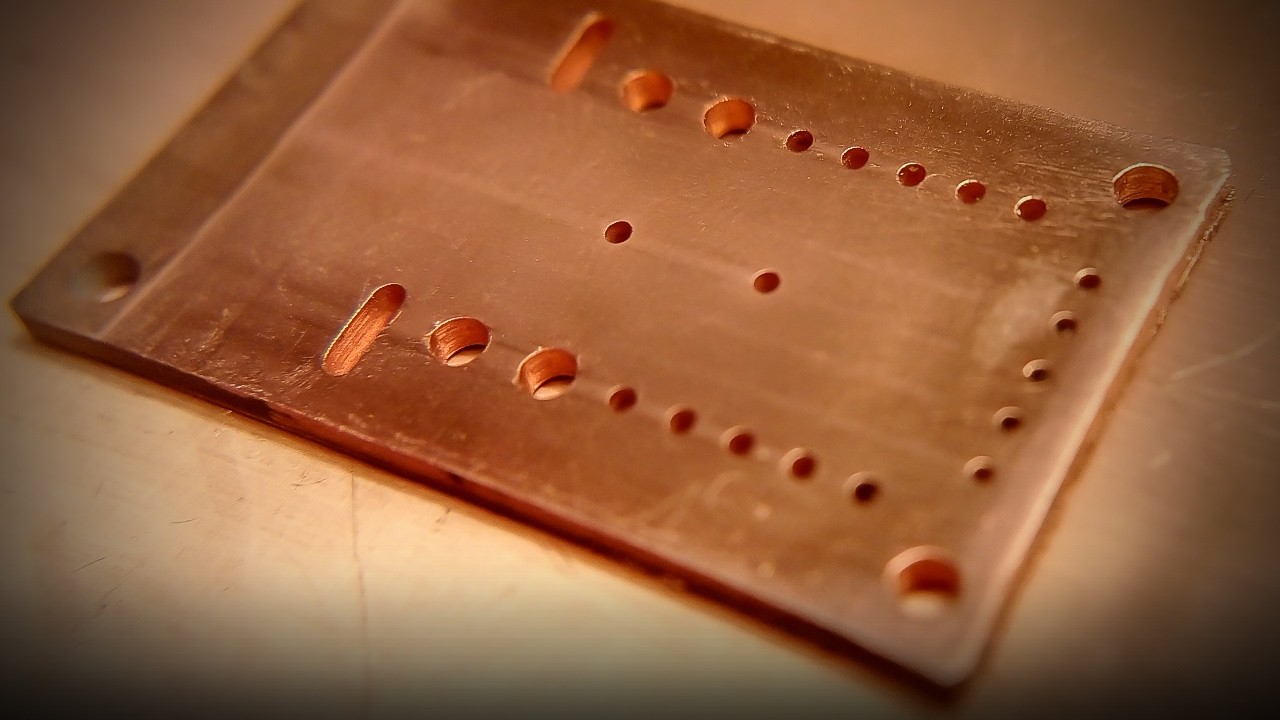
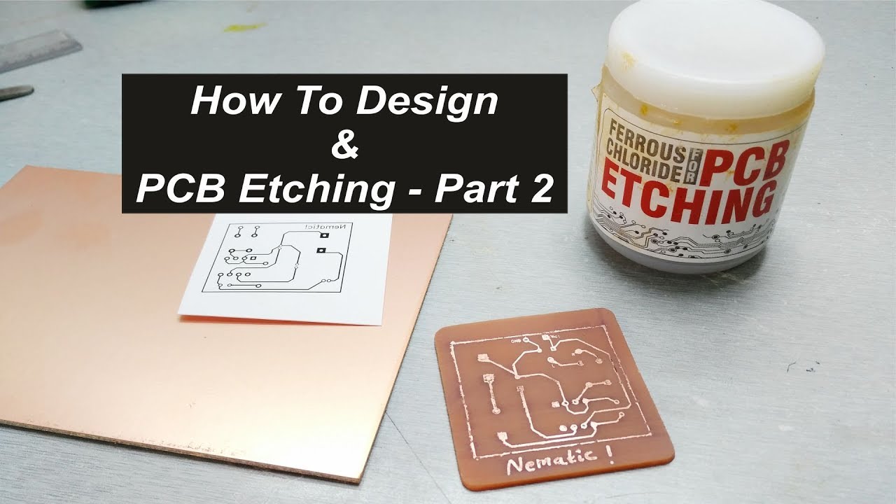
How to Design & PCB Etching- Part 2
Автор: NematicsLab
Загружено: 2018-03-28
Просмотров: 161736
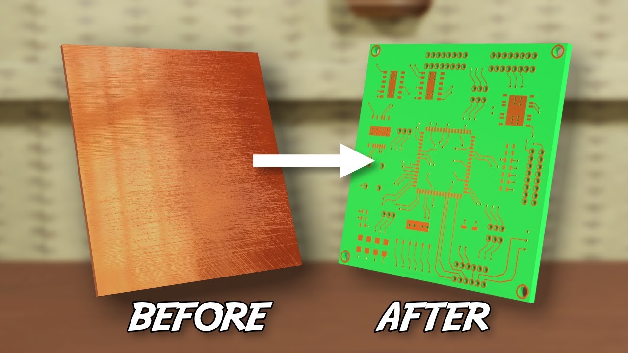
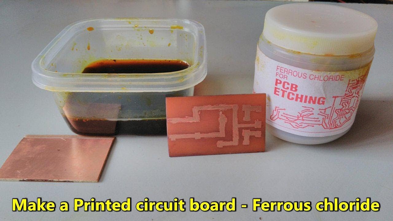
In this videos tutorial I will show you the entire process of making a PCB right from designing as well as transferring it to copper clad
More project information on Instructables:- https://www.instructables.com/id/How-...
Website,
https://NematicsLab.com
Patreon,
/ nematicslab
For Sponsorships or Endorsements ONLY!
Business@Nematicslab.com
For project-related questions use Facebook or Twitter @NematicsLab
Electronics Starter kit Tools:
Soldering Iron - https://www.banggood.in/custlink/DKGK...
Solder wire - https://www.banggood.in/custlink/mv3v...
Helping Hands - https://www.banggood.in/custlink/vmvm...
Hot Glue - https://www.banggood.in/custlink/D3GD...
Music: Doing Just Fine
link: / lakeyinspired
--------- Affiliate ---------
Gearbest- http://bit.ly/2KD54KD
Banggod- http://bit.ly/2xgJIK5
LCSC - http://bit.ly/2KD0hJ0
--------- Social Media ---------
Facebook - http://bit.ly/2FC5lJz
Instagram - http://bit.ly/2XddQpe
Twitter - http://bit.ly/2IUhqMm
Доступные форматы для скачивания:
Скачать видео mp4
-
Информация по загрузке: