Популярное

Музыка Кино и Анимация Автомобили Животные Спорт Путешествия Игры Юмор

Интересные видео

2025 Сериалы Трейлеры Новости Как сделать Видеоуроки Diy своими руками

Топ запросов

смотреть а4 schoolboy runaway турецкий сериал смотреть мультфильмы эдисон
dTub
Скачать

PCB Design for minimising Electromagnetic interference

Автор: Croydon EMC Solutions

Загружено: 2020-04-02

Просмотров: 13180

Описание:

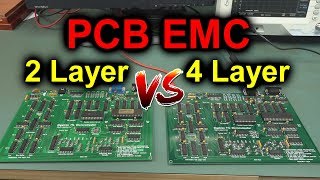
Much of electromagnetic interference challenges can be contained by designing the PCB effectively. There are a handful of techniques that needs to be followed for significant improvement in the electromagnetic performance of your device. This video explains the important parameters that need to be considered in your design for Electromagnetic Compatibility

PCB Design for minimising Electromagnetic interference

Поделиться в:

Доступные форматы для скачивания:

Скачать видео mp4

  • Информация по загрузке:

Скачать аудио mp3

Похожие видео

Flawless PCB design: RF rules of thumb - Part 1

Flawless PCB design: RF rules of thumb - Part 1

Understanding Signal Integrity

Understanding Signal Integrity

Checking into Silicon city HF Net and qso on 40M band.

Checking into Silicon city HF Net and qso on 40M band.

Electromagnetic Interference & How to Reduce it

Electromagnetic Interference & How to Reduce it

EEVblog #1176 - 2 Layer vs 4 Layer PCB EMC TESTED!

EEVblog #1176 - 2 Layer vs 4 Layer PCB EMC TESTED!

Introduction - PCB design for good EMC

Introduction - PCB design for good EMC

What Every PCB Designer Should Know - Return Current Path (with Eric Bogatin)

What Every PCB Designer Should Know - Return Current Path (with Eric Bogatin)

Этот ПРИБОР был В КАЖДОЙ квартире СССР а ЗНАЛИ о нем ЕДИНИЦЫ

Этот ПРИБОР был В КАЖДОЙ квартире СССР а ЗНАЛИ о нем ЕДИНИЦЫ

(Sponsored) High-Speed PCB Design Tips - Phil's Lab #25

(Sponsored) High-Speed PCB Design Tips - Phil's Lab #25

High Speed and RF Design Considerations

High Speed and RF Design Considerations

Мои 10 лучших советов по проектированию печатных плат

Мои 10 лучших советов по проектированию печатных плат

Layout Tips for Radiated EMI Reduction in Your Designs

Layout Tips for Radiated EMI Reduction in Your Designs

How to Reduce Noise in PCB Design

How to Reduce Noise in PCB Design

Circuit Board Layout for EMC: Example 3

Circuit Board Layout for EMC: Example 3

Ground Considerations for PCB Layout of Mixed Signal Designs Part 1

Ground Considerations for PCB Layout of Mixed Signal Designs Part 1

Switching Power Supply PCB Layout Seminar

Switching Power Supply PCB Layout Seminar

Circuit Board Layout for EMC: Example 2

Circuit Board Layout for EMC: Example 2

PCB Layout Fundamentals

PCB Layout Fundamentals

Power Distribution Tips To Control SI, EMI and Noise-Rick Hartley

Power Distribution Tips To Control SI, EMI and Noise-Rick Hartley

Поместите батарейку на магнит — результат вас удивит! 😱 | Секрет изобретателя

Поместите батарейку на магнит — результат вас удивит! 😱 | Секрет изобретателя

© 2025 dtub. Все права защищены.


  • Контакты
  • О нас
  • Политика конфиденциальности


Контакты для правообладателей: [email protected]