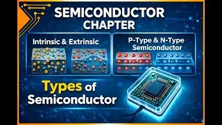
#semiconductors
Автор: IITian Neeraj Kushwaha
Загружено: 2026-01-17
Просмотров: 10
#semiconductors #class12 #physics #pnjunction diode
PN Junction Diode – Complete Explanation (Class 12 Physics)
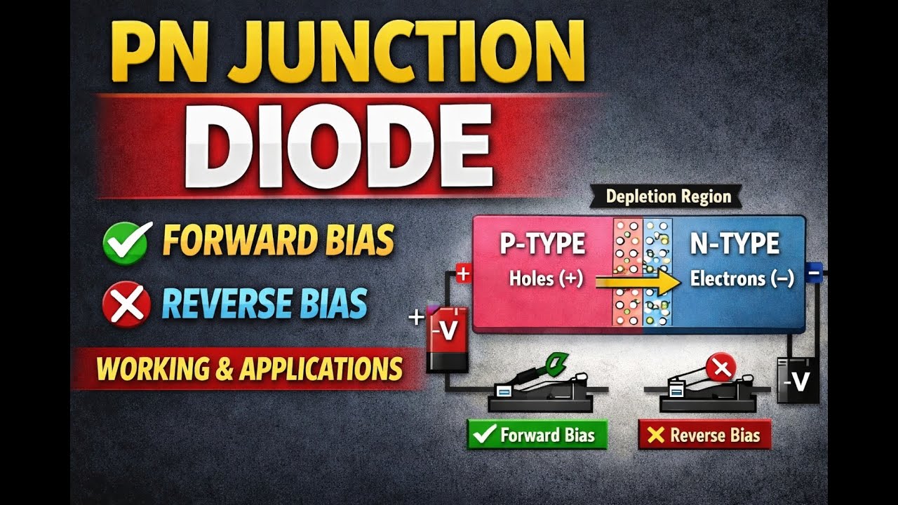
A PN junction diode is one of the most important semiconductor devices in electronics. It is formed when a p-type semiconductor is joined with an n-type semiconductor in a single crystal.
Formation of PN Junction
P-type semiconductor is doped with trivalent impurities and has holes as majority charge carriers.
N-type semiconductor is doped with pentavalent impurities and has electrons as majority charge carriers.
When p-type and n-type regions are joined, charge carriers diffuse across the junction.
Depletion Region
Electrons from the n-side recombine with holes from the p-side near the junction.
This creates a region free of mobile charge carriers called the depletion layer.
An internal electric field is developed, creating a potential barrier that opposes further diffusion.
Biasing of PN Junction Diode
Forward Bias
P-side connected to positive terminal and n-side to negative terminal.
Depletion region width decreases.
Potential barrier reduces.
Current flows easily through the diode.
Diode behaves like a closed switch.
Reverse Bias
P-side connected to negative terminal and n-side to positive terminal.
Depletion region widens.
Potential barrier increases.
Very small current flows (reverse saturation current).
Diode behaves like an open switch.
V–I Characteristics
In forward bias, current increases rapidly after a certain voltage:
0.7 V for silicon
0.3 V for germanium
In reverse bias, current remains almost constant until breakdown occurs.
Applications of PN Junction Diode
Rectifiers (AC to DC conversion)
Signal demodulation
Voltage regulation
Electronic switching circuits
Conclusion
The PN junction diode allows current to flow only in one direction, making it a fundamental building block of modern electronic devices.
Доступные форматы для скачивания:
Скачать видео mp4
-
Информация по загрузке: